
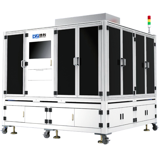
PCB AVI(Automatic Visual Inspection)

  • High-Efficiency Inspection: Simultaneous double-sided inspection, automatic board alignment and focusing, and rapid localization of circuit defects
    Intelligent Algorithm: AI deep learning enables filtering of texture/reflection interference, reducing inspection omissions and misjudgments
    Flexible Layout: Adopting a modular design, it supports online material feeding/discharging or standalone operation, and is compatible with automatic loading and unloading
    Full-Process Tracing: Inspection data is saved and exported in real time, providing a basis for process improvement and quality management
    Precise Recognition: Equipped with a high-definition line-scan color CCD, and multi-angle light sources to highlight circuit details
    Multi-Functional Configuration: Standard-equipped with laser marking, realizing the integration of inspection and tracing
    Easy Operation: Intelligent parameter adjustment and dimming, significantly shortening the training time for new operators and reducing the burden of manual inspection
    High-Precision Inspection: Special light sources combined with AI deep learning algorithms enable accurate identification of invisible surface defects, effectively reducing the misjudgment rate
    High-Speed Production Capacity: Uninterrupted loading and unloading, flexible switching between single-panel and double-panel inspection, improving inspection efficiency
    Board Surface Protection: Belt-type transmission, no scratch on the board surface, simple maintenance, and reduced costs
    Data Empowerment: Capable of connecting with systems such as MES, with real-time upload, analysis and tracing of inspection data, facilitating the digital upgrading of production
    Optical Configuration: High-resolution color CCD + ultra-high brightness LED multi-directional light sources, ensuring stable output of inspection images

Share to
High-Efficiency Inspection: Simultaneous double-sided inspection, automatic board alignment and focusing, and rapid localization of circuit defects
Intelligent Algorithm: AI deep learning enables filtering of texture/reflection interference, reducing inspection omissions and misjudgments
Flexible Layout: Adopting a modular design, it supports online material feeding/discharging or standalone operation, and is compatible with automatic loading and unloading
Full-Process Tracing: Inspection data is saved and exported in real time, providing a basis for process improvement and quality management
Precise Recognition: Equipped with a high-definition line-scan color CCD, and multi-angle light sources to highlight circuit details
Multi-Functional Configuration: Standard-equipped with laser marking, realizing the integration of inspection and tracing
Easy Operation: Intelligent parameter adjustment and dimming, significantly shortening the training time for new operators and reducing the burden of manual inspection
High-Precision Inspection: Special light sources combined with AI deep learning algorithms enable accurate identification of invisible surface defects, effectively reducing the misjudgment rate
High-Speed Production Capacity: Uninterrupted loading and unloading, flexible switching between single-panel and double-panel inspection, improving inspection efficiency
Board Surface Protection: Belt-type transmission, no scratch on the board surface, simple maintenance, and reduced costs
Data Empowerment: Capable of connecting with systems such as MES, with real-time upload, analysis and tracing of inspection data, facilitating the digital upgrading of production
Optical Configuration: High-resolution color CCD + ultra-high brightness LED multi-directional light sources, ensuring stable output of inspection images

Related Products

Contact Now

* We respect your privacy. When you submit your contact information, we agree to only contact you in accordance with our Privacy Policy.

Inquire Now

* We respect your privacy. When you submit your contact information, we agree to only contact you in accordance with our Privacy Policy.